The ALS-U project plan has now been updated, and we have revised our proposal calls leading up to the dark time. Dark time remains on track to start no earlier than October 2027 (~22 months). With substantial user beamtime anticipated in 2027, we’ve added a new proposal call due September 2, 2026. Learn more about the details and contact alsproposals@lbl.gov with questions. Read more »
A World of Vibe Coding Opportunities at the ALS
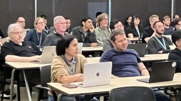
In April 2026, a panel of vibe coders hosted a tutorial at the ALS. From a general overview to specific strategies to optimize the code, participants learned all about how vibe coding can improve their workflows. Read more »
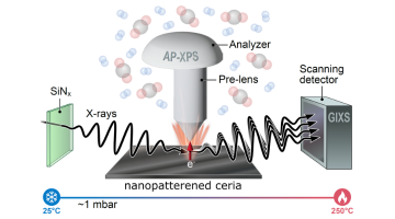
Seeing Double: Dual Measurements of Ceria Provide Insights for Catalysis
In a recent study at the ALS, researchers employed an approach that combines two techniques and uses a single X-ray beam to capture both chemical and structural changes in nanopatterned ceria during catalytic reactions. Read more »
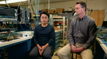
ALS-United: Changchun Sun and Jonah Weber
ALS-United is an opportunity to meet the people collaborating at the Advanced Light Source and the ALS Upgrade Project. Hear firsthand how team science enables the cutting-edge research of today and builds the facility of the future. This month, we spoke with Changchun Sun (Staff Scientists/Engineer) and Jonah Weber (Electronics Engineer). Read more »
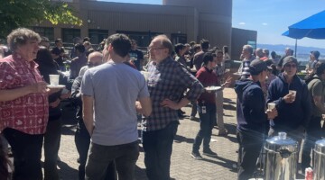
Poster Session for Spring 2025 Cohort of ALS Fellows
On the sunny afternoon of April 23, the ALS community gathered to celebrate a year of excellent science from the ALS fellows. The Spring 2025 Cohort presented their posters, and everyone enjoyed cake on the patio. Read more »